SPI, or Serial Peripheral Interface, is a classic and ubiquitous communication method between microcontrollers, sensors, and other integrated circuits.
Main Intuition: SPI is just a single shift register stretched across space. The controller shift register and peripheral shift register form a continuous circular ring. Every clock pulse pushes a bit from Controller -> Peripheral while simultaneously pulling a bit from Peripheral -> Controller.
Developed by Motorola in the 1980s, SPI was designed for maximum speed and physical simplicity. Unlike I2C or CAN, SPI skips arbitration, addressing, packet structures, and error checking. By removing protocol overhead, SPI can easily run from a few hundred kHz up to 50+ MHz.
Physical Pins
SPI uses 4 signals:
SCK(Serial Clock): Generated solely by the master controller.MOSI/COPI(Master Out Slave In / Controller Out Peripheral In): Data shifted from master to slave.MISO/CIPO(Master In Slave Out / Controller In Peripheral Out): Data shifted from slave to master.CS/SS(Chip Select / Slave Select): Active-LOW signal driven by the master to select a target peripheral.
Note on Naming: To phase out legacy master/slave terminology, modern datasheets increasingly use COPI/CIPO or SDO/SDI (Serial Data Out / Serial Data In).
Topologies
SPI is fundamentally a point-to-point connection between a controller and peripheral. Unlike buses such as I2C, SPI does not define device addresses or arbitration. The controller selects the peripheral by controlling its Chip Select (CS) line.
Because SPI is so simple, there are several common ways to connect multiple peripherals.
Single Peripheral
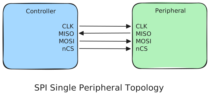
The simplest SPI configuration connects one controller to one peripheral. The clock and data signals are shared directly:
SCK: Controller -> PeripheralMOSI: Controller -> PeripheralMISO: Peripheral -> ControllerCS: Controller -> Peripheral
Since there is only one possible target, the CS line is sometimes tied permanently LOW (i.e., always active). This is common for simple devices that are always selected.
Multiple Peripherals
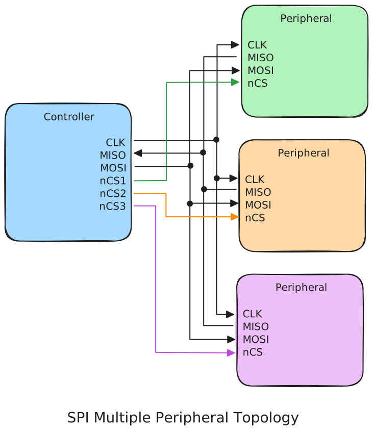
The most common SPI topology connects multiple peripherals to the same clock and data lines.
All peripherals share SCK, MOSI, MISO. However, each peripheral requires its own CS line. The controller communicates with exactly one peripheral at a time by pulling its CS line LOW. Every other peripheral must release its MISO output by entering a high-impedance state.
This topology is simple and flexible, but it requires one GPIO pin per peripheral.
Daisy-Chained Peripherals
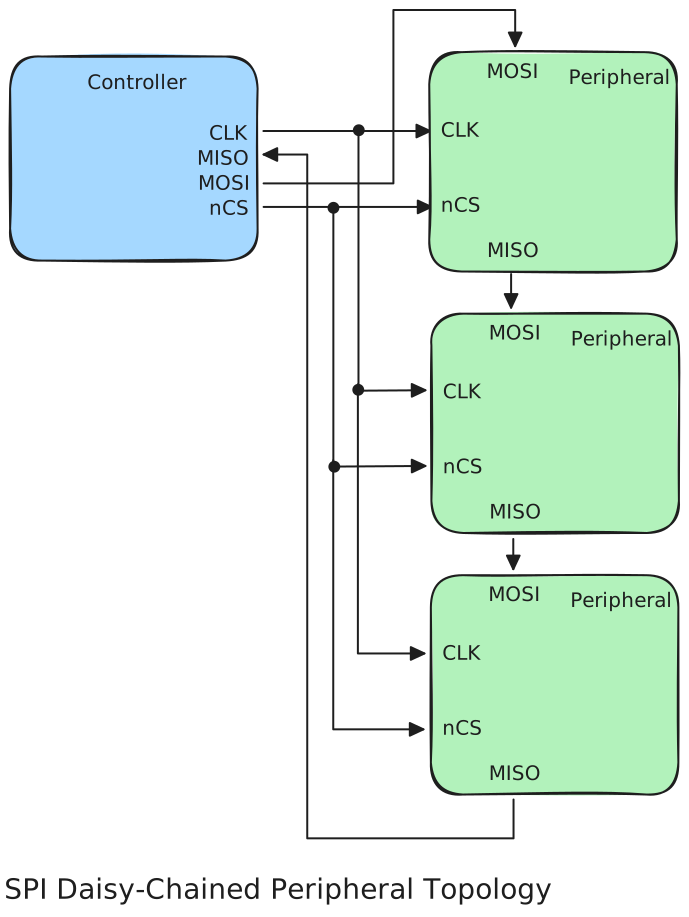
Some SPI devices support daisy chaining by connecting the output of one device to the input of the next.
Internally, each peripheral behaves like a section of a larger shift register. Data shifted into the first device propagates through every device before returning to the controller.
The advantage is that many devices can be controlled using a single CS line. The disadvantage is that every transaction must include enough clock cycles to shift data through every device in the chain.
For example, if three 8-bit devices are daisy chained, the controller must transmit 24 clock cycles to update all three devices.
Daisy chaining is common in devices such as LED drivers, display controllers, and shift-register expanders where identical devices need to receive long streams of configuration data.
Understanding Clock Polarity (CPOL) and Phase (CPHA)
Because SPI lacks an official standard, manufacturers choose their own clocking behavior. To ensure two chips talk, you must align CPOL and CPHA:
- CPOL (Clock Polarity): Defines the idle state of SCK when no data is being transferred.
CPOL = 0: SCK idles LOW.CPOL = 1: SCK idles HIGH.
- CPHA (Clock Phase): Defines which clock edge samples (reads) data.
CPHA = 0: Data is sampled on the 1st clock edge (leading edge) and shifted on the 2nd edge.CPHA = 1: Data is shifted on the 1st clock edge and sampled on the 2nd clock edge (trailing edge).
The 4 SPI Modes
| Mode | CPOL | CPHA | Clock Idle | Sample Edge | Shift Edge |
|---|---|---|---|---|---|
| Mode 0 | 0 | 0 | LOW | 1st | 2nd |
| Mode 1 | 0 | 1 | LOW | 2nd | 1st |
| Mode 2 | 1 | 0 | HIGH | 1st | 2nd |
| Mode 3 | 1 | 1 | HIGH | 2nd | 1st |
Many guides/datasheets focus on the rising/falling of the clock when discussing CPOL/CPHA. This leads to significant confusion as the rise/fall behavior changes due to CPOL! A simpler way to understand this is by looking at the “phase” of the clock waveform. CPOL simply defines the idle state, while CPHA defines the edge number to sample/shift.
The following timing diagrams show an example SPI waveform between a microcontroller and some peripheral. To keep things simple, the microcontroller sends 4 bits out, and the peripheral responds with 4 bits. Note that MOSI and MISO can have bits traveling on them simultaneously, but the diagrams have kept them sequential to avoid any confusion. Likewise, all propagation delays have been omitted.
Mode 0 (CPOL=0, CPHA=0)

In this configuration, the clock is LOW by default (CPOL=0). Sampling is done on the first clock edge and data is shifted out on the second clock edge (CPHA=0). Both microcontroller and sensor follow this scheme (the microcontroller samples/shifts on MOSI while the sensor samples/shifts on MISO). Most importantly, a clock must be provided by the microcontroller during the entire transaction.
Mode 1 (CPOL=0, CPHA=1)

In this configuration, the clock remains LOW by default (CPOL=0). Unlike Mode 0, data is shifted out on the first edge and sampling is done on the second edge (CPHA=1).
Mode 2 (CPOL=1, CPHA=0)

Mode 2 is very similar to Mode 0, except that the clock is HIGH by default (CPOL=1). Sampling is done on the first clock edge and data is shifted out on the second clock edge (CPHA=0).
Mode 3 (CPOL=1, CPHA=1)

In this configuration, the clock remains HIGH by default (CPOL=1). Data is shifted out on the first edge and sampling is done on the second edge (CPHA=1).
Timing Requirements
While SPI does not have a required frequency, each component on the bus has three critical timing requirements specified in its datasheet for reliable operation:
- Setup Time: The minimum amount of time a data signal (
MISO/MOSI) must be stable before the clock edge that samples it. - Hold Time: The minimum amount of time a data signal (
MISO/MOSI) must remain stable after the sampling clock edge. - Delay Time: The required time between a Chip Select (
CS) transition and the first (or last) clock edge.
Setup Time
Setup time is the interval between a data transition and the clock edge that samples it. If the data line is still transitioning when the receiver samples it, the sampled value may be incorrect or undefined. Meeting the setup time requirement ensures the receiver sees a stable logic level before making its decision.
Hold Time
Hold time is the interval after the sampling clock edge during which the data line must remain unchanged. If the transmitting device changes the data too soon after the clock edge, the receiver may not have enough time to reliably latch the correct value. Satisfying the hold time requirement guarantees the sampled bit is captured correctly.
Delay Time
Delay time defines how long the bus must wait after Chip Select (CS) is asserted before clocking data, and in some devices how long CS must remain asserted after the final clock edge. This gives the peripheral time to recognize that it has been selected and prepare its internal circuitry for communication. Violating this timing can cause the first bit or even the entire transaction to be missed.
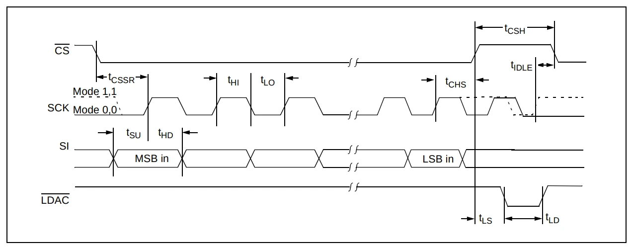
The timing diagram below shows an example SPI transaction with an MCP4921 12-bit DAC. We can see that the device operates on SPI Mode 1 (clock idle LOW, data sampled on the first edge, shifted on the second edge). t_su is the setup time, t_hd is the hold time, and t_cssr is the delay time.
Things I Wish Someone Told Me
SPI is a distributed shift register
The easiest way to understand SPI is to forget about “sending bytes” and instead think about two shift registers connected together.
Every clock pulse causes both devices to shift by one bit:
- One bit moves from the controller’s shift register into the peripheral.
- One bit moves from the peripheral’s shift register into the controller.
This means SPI is inherently full duplex. A controller can transmit and receive data simultaneously, even if one direction is ignored by the application.
Daisy chaining works because multiple peripherals can be viewed as one large shift register. Each device simply shifts incoming bits to the next device until the entire chain has received its data.
SPI isn’t a strict protocol
Unlike I2C or CAN, there is no standard frame header, device addressing, or packet length. One IC might expect an 8-bit command followed by 24-bit data; another might use 16-bit words. You must parse the device’s datasheet to write higher-level software wrappers.
Likewise, ensure that you understand how each IC drives the SPI pins. Most chips use push-pull, but some use open-drain on the MISO line! Knowing this ensures you have pullup resistors on the right pins and will save you from a significant debugging headache.
Ensure MISO isn’t left floating
If no slave CS line is active, all slaves will tristate (High-Z) their MISO output. This causes the MISO line to float, leading to strange behavior when reading the signal using a logic analyzer. Placing a pullup resistor on the line ensures it remains at a known idle state.