Preface
This tutorial dives deep into how GPIO (General Purpose Input/Output) works at the register level on the STM32. It intentionally avoids vendor HAL (Hardware Abstraction Layer) libraries and CubeMX code generation to force a complete understanding of how every individual register configures the underlying hardware.
While bare-metal register configuration takes more initial effort than calling HAL functions, mastering this process gives you precise control over your hardware and builds the necessary foundation for future peripheral drivers like SPI, I2C, and UART.
Goal
By the end of this guide, you will understand how to:
- Configure a GPIO pin as a digital input to sample a pushbutton state.
- Configure a GPIO pin as a push-pull output to drive an LED.
- Configure GPIO pins for Alternate Function mode (mapping hardware pins to SPI1).
- Use atomic register operations to read input states and drive output pins.
I’ll be using a NUCLEO-F401RE as the programming target going forward.
Note: This post focuses on configuring GPIO for STM32F4, F7, etc. It will not work for the F1 series as they use a completely different register setup!
GPIO Port vs. GPIO Pin
A common point of confusion when starting with microcontrollers is the distinction between a GPIO port and a GPIO pin.
GPIO Port
A GPIO port is a peripheral block containing a bank of up to 16 individual hardware pins managed by a shared set of configuration registers. On STM32 microcontrollers (such as the STM32F401RE found on the NUCLEO-F401RE board), GPIO ports are designated alphabetically: GPIOA, GPIOB, GPIOC, etc.
Each port maps to a 16-bit range:
GPIOA$\rightarrow$PA0toPA15GPIOB$\rightarrow$PB0toPB15GPIOC$\rightarrow$PC0toPC15
Think of a GPIO port as an entire rack of light switches.
GPIO Pin
A GPIO pin represents a single physical silicon pad routed to a pin on the chip package.
Examples:
PA5= Pin 5 on GPIO Port APB3= Pin 3 on GPIO Port BPC13= Pin 13 on GPIO Port C
To configure a pin, you must always select both its Port (to enable its clock and target the right register bank) and its Pin Index (to calculate bit shifts within those registers).
Structure of a GPIO Pin
Although GPIO pins seem simple from a software perspective, each pin routes through a flexible hardware matrix inside the silicon.
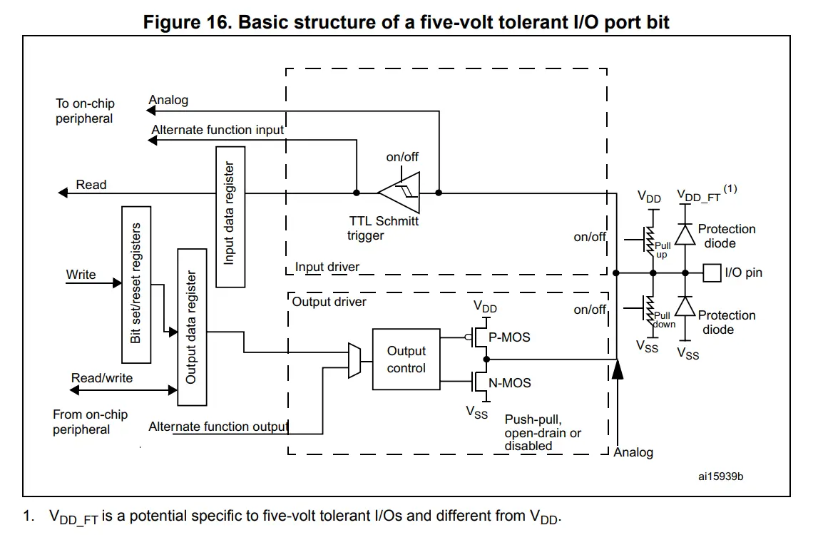
Every GPIO path contains:
- Input logic: Schmitt triggers and programmable pull-up/pull-down resistors connected to the Input Data Register (
IDR). - Output logic: Push-pull or open-drain MOSFET drivers controlled via the Output Data Register (
ODR) or Bit Set/Reset Register (BSRR). - Alternate Function multiplexers: Switches that disconnect the standard
ODR/IDRpath and connect the physical pin directly to internal hardware peripherals (SPI, I2C, USART, Timers).
Mapping Physical Pins to GPIOs
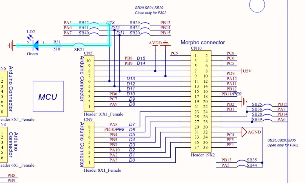
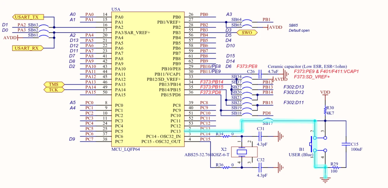
Before writing code, map physical hardware connections on your dev board using the schematic and datasheet.
For the NUCLEO-F401RE:
- User Button (B1): Connected to
PC13(Port C, Pin 13). - User LED (LD2): Connected to
PA5(Port A, Pin 5).
The Standard Register Configuration Sequence
Configuring any STM32 GPIO pin requires executing operations in a strict hardware sequence:
- Enable Peripheral Bus Clock: Gate clock power to the required GPIO port in the RCC.
- Set Mode (
MODER): Select Input, Output, Alternate Function, or Analog mode. - Configure Electrical Properties: Select Output Type (
OTYPER), Output Speed (OSPEEDR), and Pull-Up/Pull-Down resistors (PUPDR). - Map Alternate Function (
AFR): Connect internal peripherals (ifMODERis set to Alternate Function).
Step 1: Enabling Peripheral Bus Clocks
On STM32 devices, peripheral clocks are disabled by default after reset to minimize power consumption. Accessing a peripheral register before enabling its bus clock will cause silent write failures or trigger a CPU bus fault.
Check the Memory Map section in the Reference Manual (RM0368) to verify which bus owns your target GPIO ports.
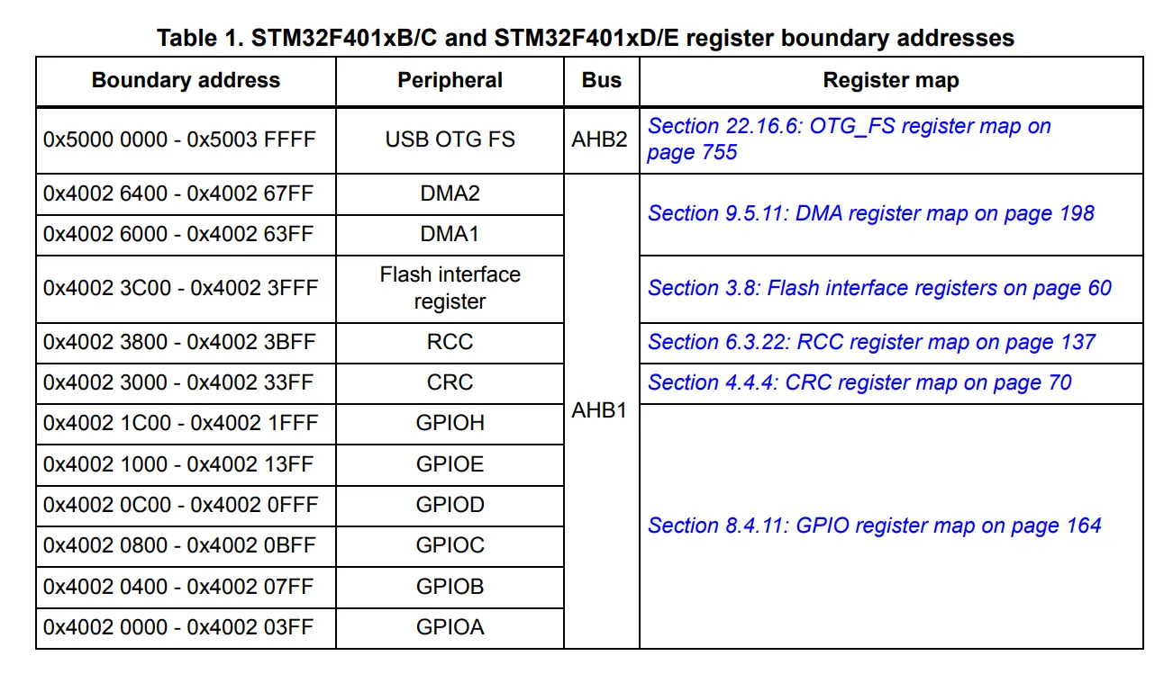
GPIOA and GPIOC reside on the AHB1 bus. Therefore, we modify the RCC_AHB1ENR register.
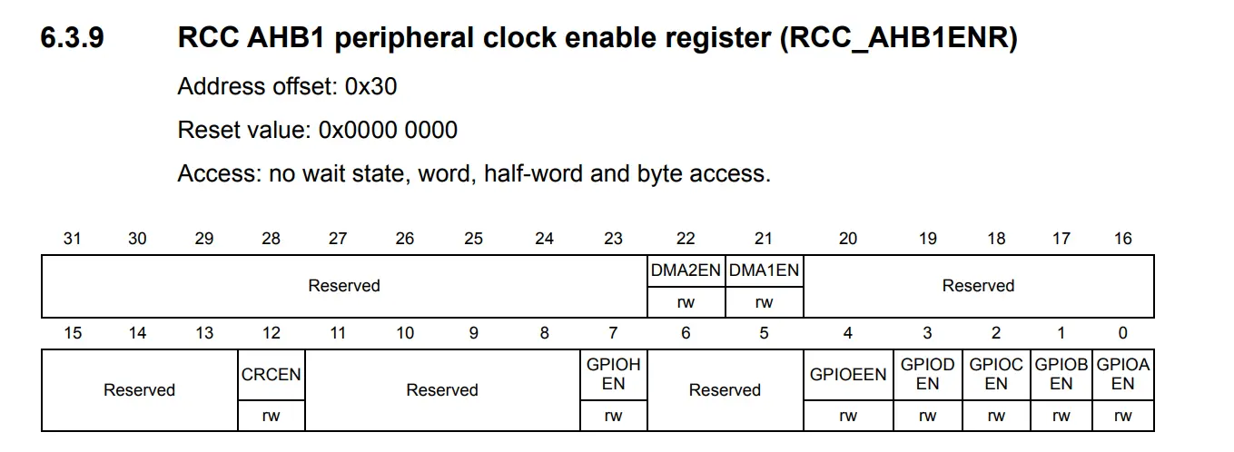
- Bit 0 (
GPIOAEN): Set to1to enableGPIOA. - Bit 2 (
GPIOCEN): Set to1to enableGPIOC.
// Enable GPIOA (Bit 0) and GPIOC (Bit 2) clocks simultaneously
RCC->AHB1ENR |= (0x1U << 0) | (0x1U << 2);
Step 2: Configuring Pin Mode (GPIOx_MODER)
Each pin uses a 2-bit field in MODER to determine its fundamental operating mode:
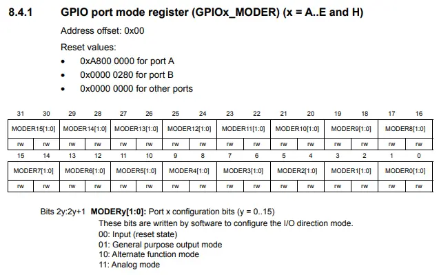
We can configure A5 as an output and PC13 as an input
// Configure PA5 as General Purpose Output (0b01)
GPIOA->MODER &= ~(0x3U << (5 * 2));
GPIOA->MODER |=  (0x1U << (5 * 2));

// Configure PC13 as Digital Input (0b00)
GPIOC->MODER &= ~(0x3U << (13 * 2));
Step 3: Configuring Electrical Properties
1. Output Type Register (GPIOx_OTYPER)
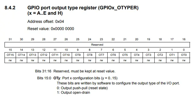
This register controls how output pins are set up. Configuring LEDs as push-pull is the simplest approach. C13 can be skipped as it is an input.
// Set PA5 to Push-Pull mode (0b0)
GPIOA->OTYPER &= ~(0x1U << 5);
2. Output Speed Register (GPIOx_OSPEEDR)
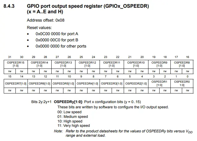
Sets output driver slew rate to limit switching noise and EMI. As the LED does not need to flash at several MHz we can set the A5 to drive at low speed.
// Set PA5 to Low Speed (0b00)
GPIOA->OSPEEDR &= ~(0x3U << (5 * 2));
3. Pull-Up / Pull-Down Register (GPIOx_PUPDR)
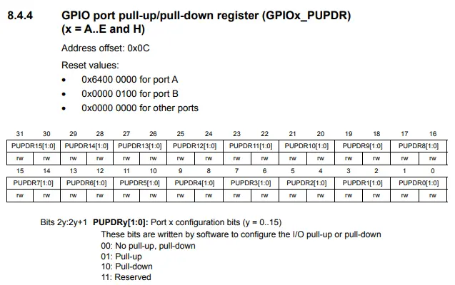
Enables internal weak pull-up or pull-down resistors. As the LED is a push-pull output and the NUCLEO has a 4.7k pullup resistor on the button, no pullups/pulldowns are needed.
// Set PA5 with no pull-up / pull-down (0b00)
GPIOA->PUPDR &= ~(0x3U << (5 * 2));

// Set PC13 with no internal pull-up / pull-down (0b00)
GPIOC->PUPDR &= ~(0x3U << (13 * 2));
Step 4: Configuring Alternate Functions (SPI Example)
Note: This is used as the initialization for our SPI peripheral in (LINK TO SPI STM32 LAB Here), where we develop a SPI controller and peripheral from scratch. We will not be using this code for this tutorial, but it goes over the concept of alternate function selection.
We can determine which pins are mapped to which peripherals using the Alternate Functions table in the datasheet. In this example we are initializing SPI1 on pins A5, A6 and A7.
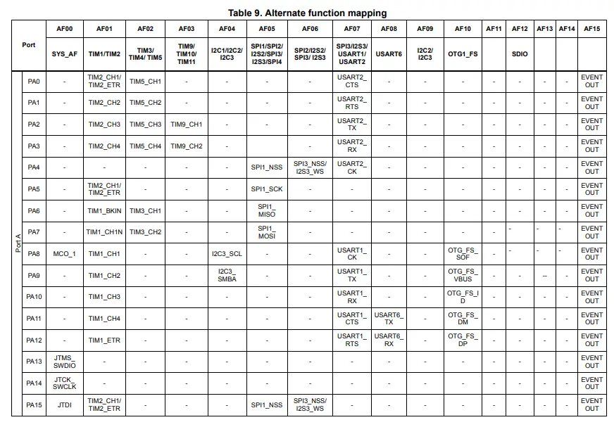
When setting a pin to Alternate Function mode (MODER = 0b10), the pin must be mapped to an internal peripheral signal using the Alternate Function registers (AFR[0] for pins 0–7, AFR[1] for pins 8–15).
Each pin occupies a 4-bit field in AFR, allowing selection from AF0 to AF15.
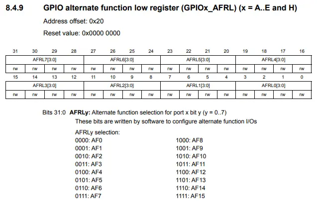
SPI1 Pin Mapping Example:
According to the STM32F401RE Datasheet Alternate Function table:
PA5$\rightarrow$SPI1_SCK(AF05)PA6$\rightarrow$SPI1_MISO(AF05)PA7$\rightarrow$SPI1_MOSI(AF05)
// 1. Set PA5, PA6, PA7 to Alternate Function Mode (0b10)
GPIOA->MODER &= ~((0x3U << (5 * 2)) | (0x3U << (6 * 2)) | (0x3U << (7 * 2)));
GPIOA->MODER |=  ((0x2U << (5 * 2)) | (0x2U << (6 * 2)) | (0x2U << (7 * 2)));

// 2. Set Output Speed to Very High for high-frequency SPI signals
GPIOA->OSPEEDR |= ((0x3U << (5 * 2)) | (0x3U << (6 * 2)) | (0x3U << (7 * 2)));

// 3. Map PA5, PA6, PA7 to AF05 in AFR[0] (AFRL - Low Register for Pins 0-7)
// Each pin takes 4 bits in AFR:
// Pin 5: shift = 5 * 4 = 20
// Pin 6: shift = 6 * 4 = 24
// Pin 7: shift = 7 * 4 = 28

// Clear existing AF selection (0xF = 0b1111)
GPIOA->AFR[0] &= ~((0xFU << (5 * 4)) | (0xFU << (6 * 4)) | (0xFU << (7 * 4)));

// Set AF05 (0x5) for PA5, PA6, PA7
GPIOA->AFR[0] |=  ((0x5U << (5 * 4)) | (0x5U << (6 * 4)) | (0x5U << (7 * 4)));
Reading an Input (GPIOx_IDR)
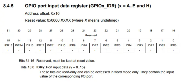
The state of every GPIO input is stored in the Input Data register. As the button is active LOW, we can write a conditional that polls this register and performs an action when C13 is LOW.
if (!(GPIOC->IDR & (0x1U << 13))) {
  // do something
}
Writing an Output (GPIOx_BSRR)
You might think that writing an output to a GPIO means setting a value to GPIOx_ODR. While this register does exist, it is the wrong one to write to! The reason why is that writes must be atomic.
The Problem with GPIOx_ODR
To change a single bit in the Output Data Register (GPIOx_ODR) without overwriting the state of other pins on the same port, you have to perform a Read-Modify-Write operation:
// Setting PA5 HIGH using ODR (NOT atomic)
GPIOA->ODR |= (1U << 5);  // Read ODR, OR-in bit 5, write back to ODR
If an interrupt or another thread executes between the Read and the Write and modifies another pin on GPIOA (say, PA2), that change will be silently overwritten and lost when your main loop finishes writing back its stale copy of ODR.
How BSRR Solves It
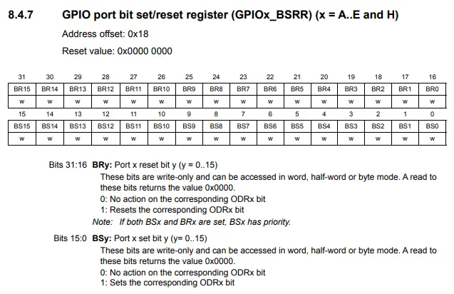
The Bit Set/Reset Register (GPIOx_BSRR) is a write-only mask register designed to solve this in hardware:
- Bits 0–15 (BS0–BS15): Writing a 1 sets the corresponding pin HIGH.
- Bits 16–31 (BR0–BR15): Writing a 1 sets the corresponding pin LOW.
Writing a 0 to any bit does nothing and leaves the pin’s state untouched.
// Set PA5 HIGH atomically
GPIOA->BSRR = (1U << 5);

// Set PA5 LOW atomically (Bit 5 + 16 = Bit 21)
GPIOA->BSRR = (1U << (5 + 16));
Because you write directly to BSRR in a single CPU instruction without reading the register first, the operation is 100% thread-safe, interrupt-safe, and enforced directly by hardware.
Putting It All Together
Here is the complete, working bare-metal C application. It configures PC13 as an input (polling the active-LOW user button) and drives PA5 (User LED) atomically using the Bit Set/Reset Register (BSRR).
#include "stm32f4xx.h"

int main(void)
{
  // Enable GPIOA and GPIOC clocks
  RCC->AHB1ENR |= (0x1U) | (0x1U << 2);

  // Set A5 as output (0b01)
  GPIOA->MODER &= ~(0x3U << (5 * 2));
  GPIOA->MODER |= (0x1U << (5 * 2));

  // Set A5 as push-pull (0b0)
  GPIOA->OTYPER &= ~(0x1U << 5);

  // Set A5 as low speed (0b00)
  GPIOA->OSPEEDR &= ~(0x3U<< (5 * 2));

  // Set A5 with no pullup (0b00)
  GPIOA->PUPDR &= ~(0x3U << (5 * 2));

  // Set C13 as input (0b00)
  GPIOC->MODER &= ~(0x3U << (13 * 2));

  // Set C13 with no pullup (0b00)
  GPIOC->PUPDR &= ~(0x3U << (13 * 2));

  while (1) {
    // Read C13 state (active LOW
    if (!(GPIOC->IDR & (0x1U << 13))) {
      // Set A5 HIG
      GPIOA->BSRR = (0x1U << 5);
    }
    else {
      // Set A5 LOW
    GPIOA->BSRR = (0x1U << 21);
    }
  }
}
Flashing and Testing
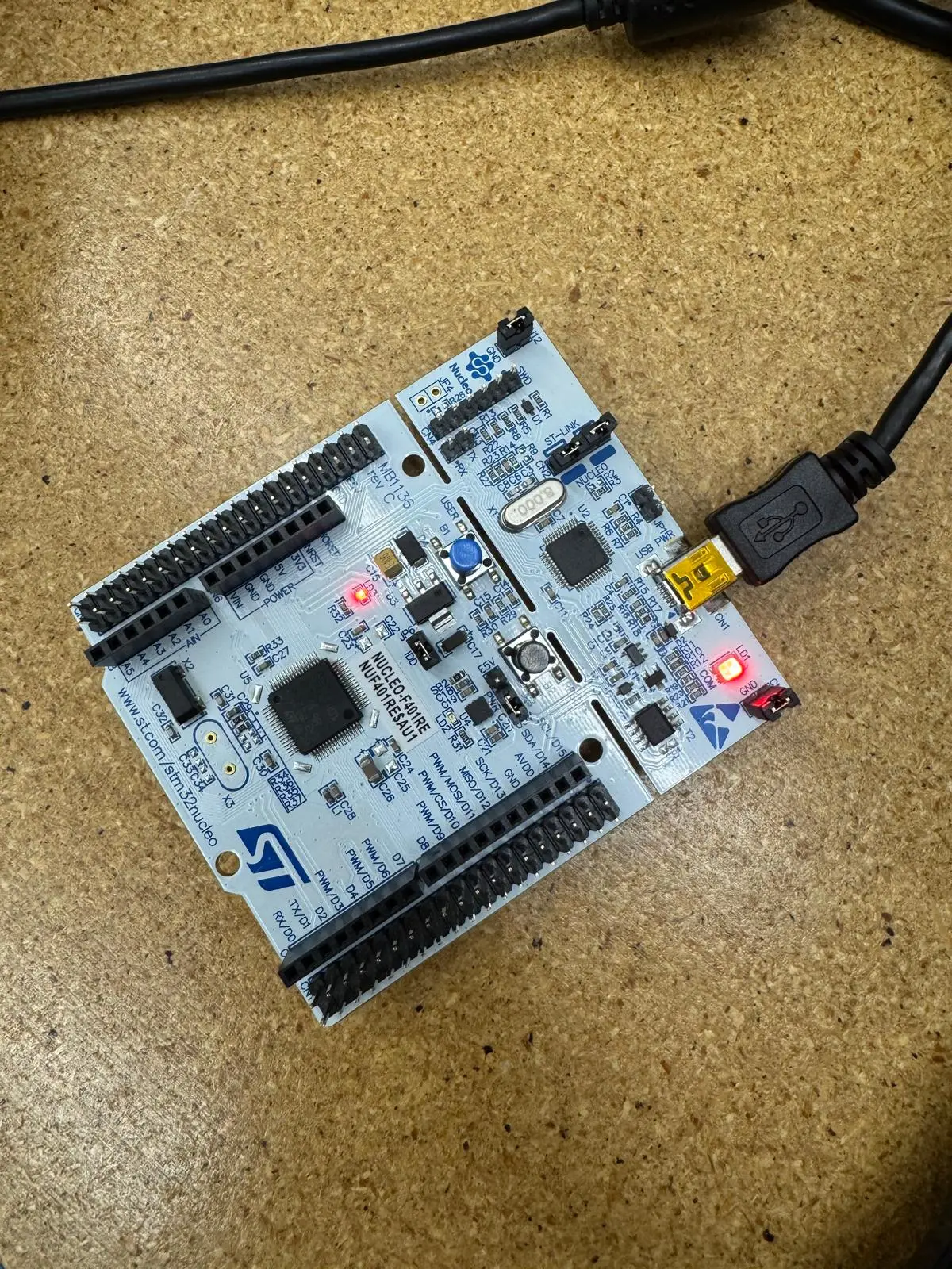
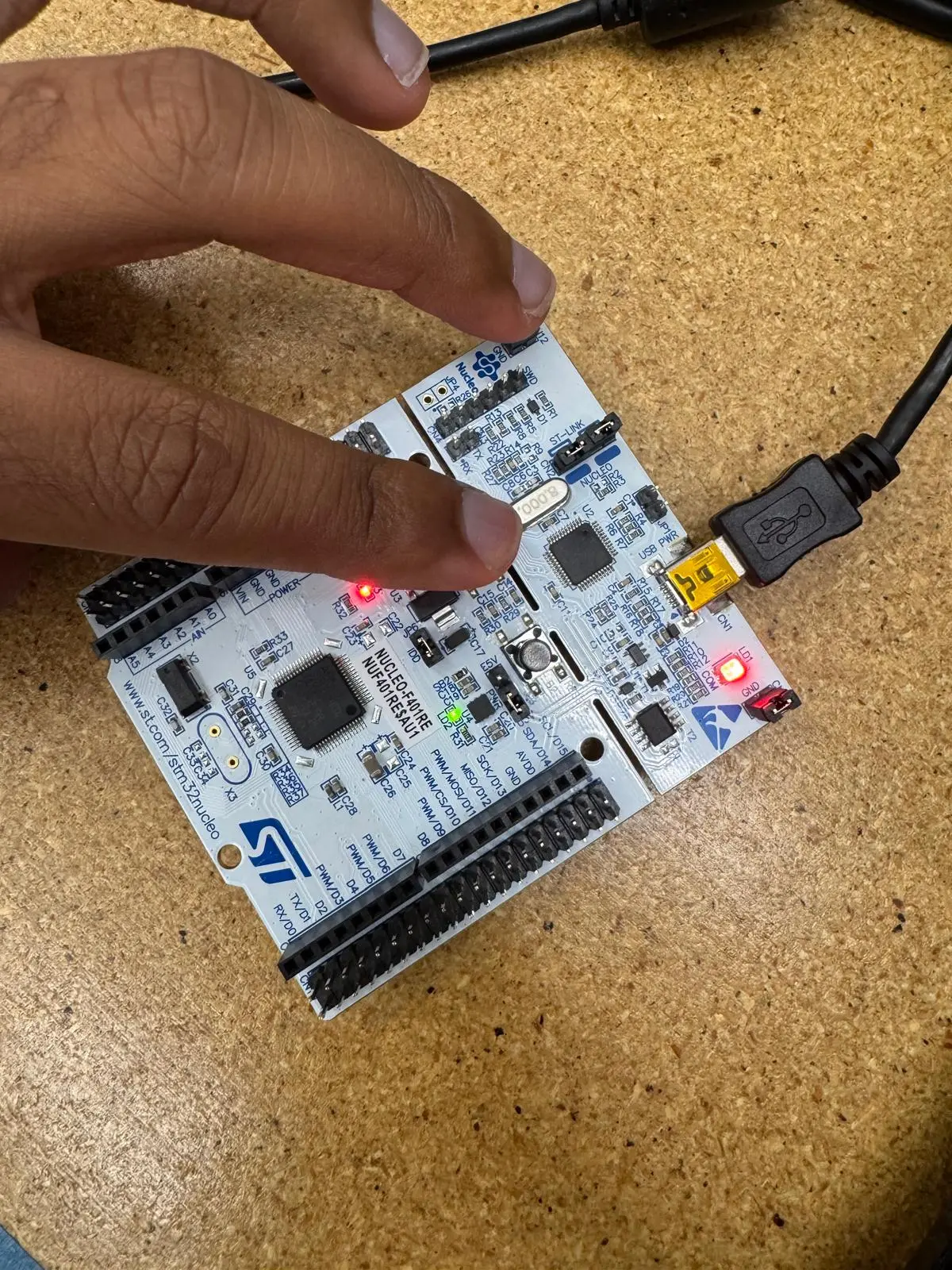
With the code complete, all thats left is to flash it to the NUCLEO and see if it worked. As expected, pressing the button lights the LED, while releasing turns it off.
Resources
Bonus: Standard CMSIS Macro Implementation
While explicit bit-shifting clarifies exact register bit geometry, CMSIS headers provide named bit constants that match the names in the STM32 Reference Manual.
Below is the identical configuration written using CMSIS definitions:
#include "stm32f4xx.h"

int main(void)
{

  // Enable GPIOA clock
  RCC->AHB1ENR |= RCC_AHB1ENR_GPIOAEN | RCC_AHB1ENR_GPIOCEN;

  // Set A5 as output (0b01)
  GPIOA->MODER &= ~GPIO_MODER_MODER5_1; // Clear bit 1
  GPIOA->MODER |= GPIO_MODER_MODER5_0;  // Set bit 0

  // Set A5 as push-pull (0b0)
  GPIOA->OTYPER &= ~GPIO_OTYPER_OT5;

  // Set A5 as low speed (0b00)
  GPIOA->OSPEEDR &= ~GPIO_OSPEEDR_OSPEED5;

  // Set A5 with no pullup (0b00)
  GPIOA->PUPDR &= ~GPIO_PUPDR_PUPD5;

  // Set C13 as input (0b00)
  GPIOC->MODER &= ~GPIO_MODER_MODER13_1;  // Clear bit 1
  GPIOC->MODER &= ~GPIO_MODER_MODER13_0;  // Clear bit 0

  // Set C13 with no pullup (0b00)
  GPIOC->PUPDR &= ~GPIO_PUPDR_PUPD13;

  while (1) {
    // Read C13 state (active LOW)
    if (!(GPIOC->IDR & GPIO_IDR_ID13)) {
      // Set A5 HIGH
      GPIOA->BSRR = GPIO_BSRR_BS5;
    }
    else {
      // Set A5 LOW
      GPIOA->BSRR = GPIO_BSRR_BR5;
    }
  }
}
Implementing the code using macros or bit-shifted values is up to the developer. Generally it is good to derive the values using bitwise operations to learn, then shift to existing macros for portability and clarity.